Jadavpur University Project Assistant Recruitment 2026 | ANRF Funded VLSI & Hardware Security Project | Walk-in Interview
The Department of Electronics & Telecommunication Engineering (ETCE), Jadavpur University, Kolkata, has announced a walk-in interview for the recruitment of Project Assistants under a prestigious ANRF (Anusandhan National Research Foundation) funded research project.
The project focuses on Hardware Security Techniques for Multi-Chiplet Systems-in-Packages, a rapidly emerging research area combining VLSI design, FPGA implementation, semiconductor systems, and cybersecurity.
This opportunity is ideal for candidates interested in VLSI, IC design, FPGA development, semiconductor technologies, and hardware security research.
About the Project
Project Title
Development of Hardware Based Security Techniques for Multi-Chiplet Systems-in-Packages
Funding Agency
ANRF (Government of India)
Sanction Order
ANRF/ARG/2025/009853/ENS
Principal Investigator (PI)
Prof. Joydeep Basu
Co-Principal Investigator (Co-PI)
Prof. Jaydeb Bhaumik
Department
Electronics & Telecommunication Engineering (ETCE)
Institution
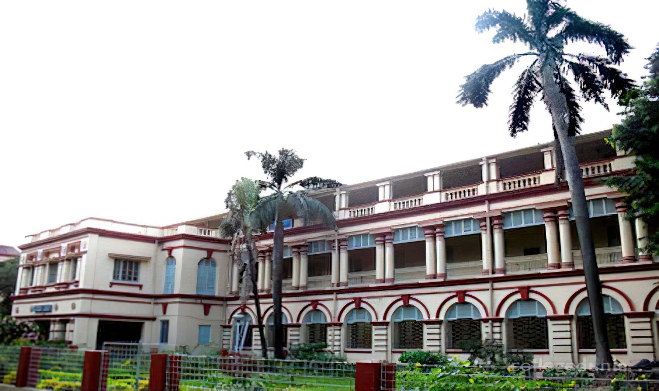
Jadavpur University, Kolkata
Recruitment Overview
| Particular | Details |
|---|---|
| Organization | Jadavpur University |
| Department | Electronics & Telecommunication Engineering (ETCE) |
| Post Name | Project Assistant |
| Number of Posts | 02 |
| Funding Agency | ANRF |
| Selection Mode | Walk-in Interview |
| Interview Date | 02 July 2026 |
| Location | Kolkata, West Bengal |
Vacancy Details
| Post | Vacancies |
|---|---|
| Project Assistant | 02 |
Essential Qualification
Candidates should possess any one of the following qualifications:
- Bachelor's Degree in Science
OR
- Three-Year Diploma in Engineering and Technology
(as per ANRF Office Memorandum ANRF/OM/N-01/2024)
Desirable Qualification
Preference will be given to candidates having:
Educational Background
- B.E./B.Tech.
- M.E./M.Tech.
in any of the following disciplines:
- Electronics & Communication Engineering
- VLSI Engineering
- Electrical Engineering
- Instrumentation Engineering
- Related Disciplines
Technical Skills
Experience in:
- Analog IC Design
- Digital IC Design
- VLSI Circuit Design
- Cadence Design Tools
- Synopsys EDA Tools
- FPGA-Based Design
- Hardware Security Applications
- Semiconductor Systems
Fellowship / Salary
Monthly Fellowship
| Component | Amount |
|---|---|
| Fellowship | ₹27,000 |
| HRA (30%) | ₹8,100 |
| Total | ₹35,100 per month |
Age Limit
Maximum Age: 50 Years
(as on the date of advertisement)
Age Relaxation
Relaxation is applicable for:
- SC Candidates
- ST Candidates
- OBC Candidates
- Women Candidates
as per Government of India rules.
Project Duration
The project will continue:
- Till completion of the project
- Maximum duration up to 48 months
Initial Appointment
- Initially for 1 Year
-
Extendable based on:
- Satisfactory Performance
- Project Requirements
- Availability of Funding
Benefits for Selected Candidates
Research Exposure
Selected candidates will gain hands-on experience in:
- VLSI Design
- FPGA-Based Circuit Design
- Hardware Security
- Semiconductor Chip Design
- IC Fabrication and Testing
- Advanced EDA Tools
Academic Growth
- Opportunity to pursue Ph.D. as per university rules
- Exposure to cutting-edge semiconductor research
- Collaboration with experienced faculty and researchers
Selection Process
Mode of Selection
Walk-in Interview
Candidates will be evaluated based on:
- Academic Performance
- Technical Knowledge
- Research Aptitude
- Interview Performance
Walk-in Interview Details
Date
📅 02 July 2026 (Thursday)
Time
🕐 1:00 PM
Venue
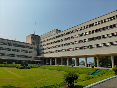
Committee Room, ETCE Department
Prayukti Bhavan
Jadavpur University
188 Raja S.C. Mallick Road
Kolkata – 700032
How to Apply?
Step 1
Obtain the prescribed application form from the Information Section of Jadavpur University.
Step 2
Fill the application form carefully.
Step 3
Bring the following documents at the time of interview:
- Original Certificates
- Mark Sheets
- Testimonials
- Experience Certificates (if any)
- Self-attested Photocopies of Documents
- Completed Application Form
Step 4
Attend the walk-in interview on the scheduled date and time.
Application Form Fee
₹50
Important Instructions
- Candidates must produce originals along with self-attested copies.
- No TA/DA will be paid for attending the interview.
- Incomplete applications may be rejected.
- Candidates should ensure they satisfy all eligibility conditions before appearing.
Contact Details
For any query regarding the project:
Principal Investigator
Prof. Joydeep Basu
Co-Principal Investigator
Prof. Jaydeb Bhaumik
Subject Line: Enquiry for Project Assistant Post
Why Apply?
✅ Work on ANRF-funded semiconductor research project
✅ Exposure to VLSI and FPGA design
✅ Hands-on experience with Cadence and Synopsys tools
✅ Opportunity to work on Hardware Security Systems
✅ Fellowship of ₹35,100 per month
✅ Potential pathway toward Ph.D.
✅ Research experience at a prestigious university
Important Dates
| Event | Date |
|---|---|
| Notification Date | 18 June 2026 |
| Walk-in Interview | 02 July 2026 |
| Reporting Time | Before 1:00 PM |
Official Notification URL
Open Positions
Relevant Streams
Related Faculty & Academic
More opportunities you might be interested in